SEMICONDUCTOR FABRICATION & MICROELECTRONICS
Home / Industries / Semiconductor
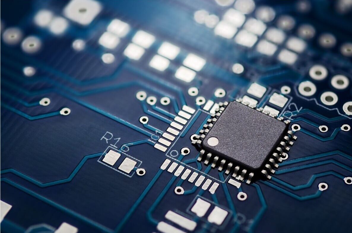
SUB-NANOMETER VIBRATION ISOLATION FOR ADVANCED NODE MANUFACTURING
The semiconductor industry represents the absolute limits of precision manufacturing. As architecture nodes shrink below 5nm, the environmental tolerances required for wafer fabrication become extraordinarily unforgiving. Even imperceptible structural vibrations or ambient acoustic pressure waves can cause severe pattern distortion during EUV lithography, misalign metrology equipment, and devastate die yields. Maya Consulting engineers the extreme active and passive vibration isolation systems required to protect your multi-billion dollar process tools, ensuring maximum uptime and flawless Class 1 cleanroom compliance.
EUV Lithography & Wafer Metrology
Advanced lithography scanners and defect inspection tools operate at sub-nanometer resolutions. These critical systems must be entirely decoupled from the Fab’s ambient kinetic energy to maintain focal precision during the multi-layer patterning process.
The Yield Risk: Micro-vibrations propagating through the Fab floor (waffle slab) cause the lithography scanner’s optical column to drift. This creates overlay errors and edge-placement defects, instantly turning a high-value wafer batch into scrap.
The Engineering Solution: We engineer dedicated, heavy-mass structural pedestals and integrate advanced active piezoelectric cancellation systems. This ensures your most sensitive tools consistently operate within the extreme VC-E to VC-G vibration criteria required by OEM specifications (like ASML).
Fab Infrastructure & Sub-Fab Decoupling
A modern Fab is a massive mechanical engine. The Sub-Fab level houses hundreds of heavy-duty vacuum pumps, massive chillers, and chemical delivery systems operating 24/7 directly beneath the pristine Class 1 cleanroom.
The Structural Risk: The continuous operation of Sub-Fab support equipment and the movement of Automated Material Handling Systems (AMHS) on the ceiling generate a constant, low-frequency hum and structural vibration that threatens the cleanroom floor above.
The Engineering Solution: We design comprehensive facility decoupling strategies. By engineering custom inertia bases for heavy Sub-Fab pumps and isolated mounting systems for AMHS tracks, we break the kinetic transmission path before vibrations can reach the critical processing level.
FAQ
COMMON QUESTIONS ABOUT SEMICONDUCTOR FAB VIBRATION & ACOUSTICS
How does ambient acoustic noise cause defects in wafer fabrication?
High-velocity cleanroom air handling units (AHUs) generate significant acoustic energy. These soundwaves act as pressure waves that strike the outer casing of sensitive tools, transferring into mechanical vibration. This can cause beam drift in electron microscopes or focal errors in lithography scanners. We engineer specialized acoustic treatments that absorb this energy without shedding particulates into the Class 1 environment.
Can you retrofit vibration isolation for a new tool installation in an active Fab?
Yes. Upgrading to a more sensitive tool (like moving from DUV to EUV lithography) often means the existing floor no longer meets the required Vibration Criterion (VC) curve. We design localized active-cancellation platforms and stiffening structures that can be installed without requiring a massive facility shutdown or concrete demolition.
Why is Sub-Fab equipment isolation so critical?
Every process tool on the cleanroom floor is supported by roughing pumps, abatement systems, and chillers located in the Sub-Fab directly below it. If these heavy mechanical systems are bolted directly to the structural columns, their vibration travels straight up to the tool. We engineer specialized spring isolators and flexible utility connections to completely decouple this support equipment.
How do you handle vibration from Automated Material Handling Systems (AMHS)?
Overhead hoists moving FOUPs (wafer carriers) across the Fab ceiling generate dynamic, shifting loads and structural vibrations that can affect the tools below them. We design specialized vibration-damping rail mounts and structural stiffening systems for the AMHS tracks to minimize kinetic transfer into the building frame.